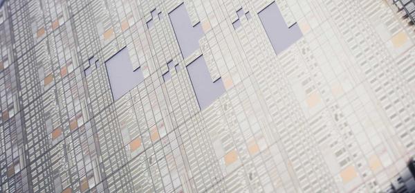
An electron micrograph on the cross section of the device manufactured on the 200mm Gan on Soi wafer.(A) is Pgan-Hemt in E mode, (b) is the d mode (Metal Insulator Semiconductor) Hemt, and (C) is a shot key barrier diode [click to enlarge]

The IMEC research team, a Belgian research institution, has raised the GAN (gallium nitride) power IC to the next level and integrates a shot key barrier diode (SBD) and HEMT (high -electronic moving transistor) on a smart power platform. Was announced. GAN Device IMEC on the wafer announced this new technology at the 2021 IEEE International Electron Devices Meeting (IEDM) held on December 11-15, 2021. The technology combines a high -performance shot key barrier diode and a blank mode mode (D mode) HEMT on the P Channel Gan HEMT -based 200V SOI (Silion on Insulator) Power IC. The platform was developed on a 200mm wafer. This combination enables design of chips with improved functionality and performance. IMEC states that "this integration will open a smaller and more efficient DC-DC converter or POL (POINT OF LOAD) converter." In an interview, Stefaan Decouter, the GAN technology program director at IMEC, improved the logic and analog function by replacing the reversal function of RTL (directly connected FET logic). They are improving the pull -up characteristics of the inverted gate. " DECOUTERE said, "GAN has no excellent P -channel device, and the degree of movement of the holes is about 1/160 of the electron, so complementary logic like CMOS is not realistic. Low voltage shot key. The diode provides functions such as level shifts and clamping with an on -tip. Using a high -voltage power shot key diode can improve the third roside switch and improve power efficiency. " 。 The next step is the development of the GAN IC prototype and the transfer to a cheaper 200mm wafer. DECOUTERE said, "In the past, GAN-ON-SI was processed with smaller diameter wafers (4 inches and 6 inches), but more and more manufacturing factories that transfer GAN technology to 200 mm." 。 The task of the larger diameter GAN-on-Si substrate is the mechanical stability of the board, considering the mismatch between the GAN / ALGAN layer and the substrate of the substrate. DECOUTERE said, "Appropriate design of buffers, such as the use of super -lattice buffers, and improving the MOCVD (organic metal chemical phase growth method) device, to deal with this mechanical stability, 200mm wafer. I realized GAN processing. " GAN HEMT is attracting attention for various purposes, such as high -frequency power amplifiers and high -voltage devices used in power electronics. In order to reduce costs and accelerate integration with SI -based components, the development of GAN HEMT using SI -based boards is currently being emphasized. However, GAN-Si interfaces often cause defects due to grid inconsistencies between GAN and SI and thermal inconsistencies. GAN HEMT has the desired number of on -resistance and performance index (FOM). Depending on the voltage and current rating, the FOM can be one -quarter to one -tenth of the Super Junction FET. As a result, GAN is very suitable for high -frequency applications. By adopting a low -on resistance GAN HEMT, conduction loss is reduced and efficiency is increased. Gan Hemt does not have a unique body diode, so there is no reverse recovery charge. The device shows various characteristics by the gate voltage, and can be revered. GAN requires a higher -speed turn -on/turn -off time (that is, faster DV/DT) and a lower, strictly managed gate -off voltage. Therefore, it is more difficult to operate the GAN device than to operate Mosfet. Optimizing the gate loop inductance, power inductance, gate register, and drain and source inductance is a major issue in operating GAN at the board level. Designers must concentrate on dead time control, DV/DT resistance, negative power supply voltage, and overcharging at the gate driver level. The symmetry of the gate driver's high side and low side is also an important factor. This is because a delay matching of less than 1 nano seconds can be realized and the dead time can be reduced. Most of the GAN power electronics are discrete parts that require an external driver IC. However, in order to make the most of the high -speed switching of GAN, integrating driver functions into monolithic devices is the key. Assuming that IMEC has improved the performance by combining e -mode (enhancement mode) and D mode HEMT devices. According to DECOUTERE, using the integrated D mode HEMT to extend the functional platform of E -mode Hemt on Soi can reduce power loss while improving speed. Another important part for integrating into GAN Power Devices is a shot key barrier diode. The shot key GAN diode has a higher reverse voltage than a silicon and a lower switching loss. According to IMEC, the GAN IC platform is available through multi -project wafer services, and partner companies can use it. First of all, in addition to a quick charger for smartphones, tablets, and laptops, it plans to develop 650V with 650V for power switching and conversion applications.
EE TIMES JAPAN